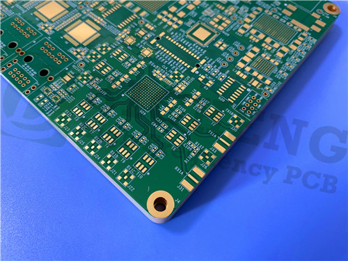
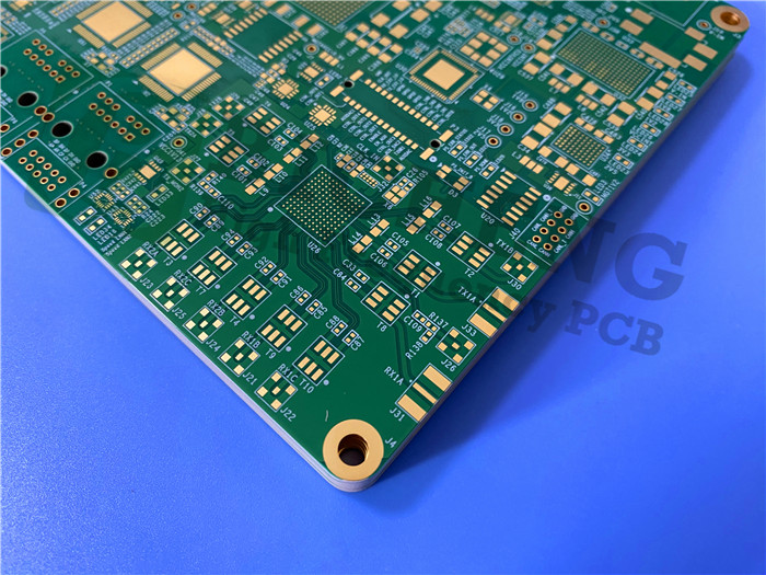
Megtron6 12-Layer 2.12mm High Speed PCB for 5G and Data Center Applications
1. Introduction of High Speed, Low Loss Multi-layer Materials - Megtron6 (M6) R-5775
The Panasonic M6 laminate is a type of multilayer copper-clad laminate (CCL) specifically designed for high-frequency, high-speed, and high-reliability electronic devices. It is applicable to fields such as 5G communication, millimeter-wave radar, high-speed servers, and high-performance computing (HPC). Its core advantages lie in low dielectric loss (Df), stable dielectric constant (Dk), and excellent thermal reliability, enabling it to meet the stringent requirements of high-frequency signal transmission.
2. Key Features
Frequency-Stable Dk: 3.4 at 1GHz/23°C, 3.34 at 13GHz
Ultra-Low Loss: Dissipation Factor of 0.002 at 1GHz/23°C, 0.0037 at 13GHz
Excellent Dimensional Stability: X axis CTE 16 ppm/°C, Y CTE 16 ppm/°C, Z CTE 45 ppm/°C
High Thermal Performance: Tg >185°C (DSC), 210°C (DMA), Td 410°C (TGA)
Multi-layer Capability: Supports 4-30 layer PCB design for complex circuits
Environmental Compliance: RoHS and halogen-free, UL 94V-0 flammability
Manufacturing Efficiency: Compatible with traditional FR-4 processing technology
3. Benefits
Optimized Performance: Combined RF and digital circuitry in single board
Enhanced Reliability: Excellent dimensional stability for mixed dielectric constructions
Cost-Effective Solution: RF performance at fraction of traditional microwave material cost
Manufacturing Efficiency: Compatible with standard processing methods
Thermal Resilience: Stable performance across wide temperature range

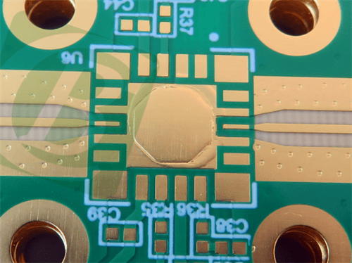
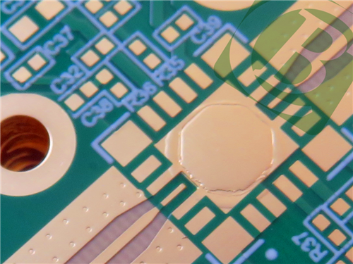
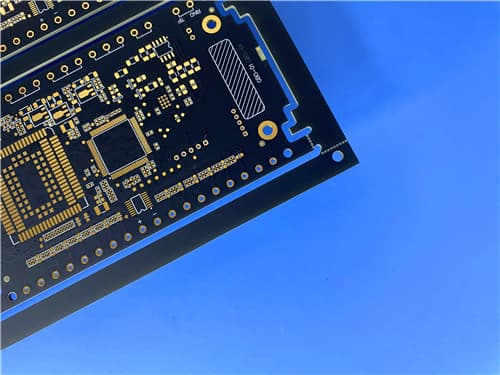
4. PCB Construction Details
| Parameter |
Specification |
| Base Material |
Megtron6 |
| Layer Count |
12 layers |
| Board Dimensions |
220mm × 60mm = 1PC, ±0.15mm |
| Minimum Trace/Space |
3/3 mils |
| Minimum Hole Size |
0.2mm |
| Blind Vias |
No |
| Finished Board Thickness |
2.12mm |
| Finished Cu Weight |
1oz outer layers, 0.5oz/1oz inner layers |
| Via Plating Thickness |
25 μm |
| Surface Finish |
ENIG |
| Top Silkscreen |
White |
| Bottom Silkscreen |
White |
| Top Solder Mask |
Blue |
| Bottom Solder Mask |
Blue |
| Via Treatment |
0.2mm, 0.4mm vias filled by resin and capped plating |
| Electrical Test |
100% tested prior to shipment |
| Design Standard |
IPC-Class-2 |
| Artwork Format |
Gerber RS-274-X |
| Availability |
Worldwide |
5. PCB Stackup (12-Layer Rigid Structure)
| Layer |
Material |
Thickness |
| Copper Layer 1 | Copper | 35 μm |
| Dielectric | Prepreg R-5670(G) 1080 (68%) ×1 | 81.4 μm |
| Copper Layer 2 | Copper | 35 μm |
| Dielectric | M6 Core R5775G(HVLP) | 75 μm |
| Copper Layer 3 | Copper | 17 μm |
| Dielectric | Prepreg R-5670(G) 3313 (59%) ×2 | 219.9 μm |
| Copper Layer 4 | Copper | 17 μm |
| Dielectric | M6 Core R5775G(HVLP) | 75 μm |
| Copper Layer 5 | Copper | 17 μm |
| Dielectric | Prepreg R-5670(G) 3313 (59%) ×2 | 216.5 μm |
| Copper Layer 6 | Copper | 35 μm |
| Dielectric | M6 Core R5775G(HVLP) | 400 μm |
| Copper Layer 7 | Copper | 35 μm |
| Dielectric | Prepreg R-5670(G) 3313 (59%) ×2 | 215.6 μm |
| Copper Layer 8 | Copper | 17 μm |
| Dielectric | M6 Core R5775G(HVLP) | 75 μm |
| Copper Layer 9 | Copper | 17 μm |
| Dielectric | Prepreg R-5670(G) 3313 (59%) ×2 | 219.8 μm |
| Copper Layer 10 | Copper | 17 μm |
| Dielectric | M6 Core R5775G(HVLP) | 75 μm |
| Copper Layer 11 | Copper | 35 μm |
| Dielectric | Prepreg R-5670(G) 1080 (68%) ×1 | 81.4 μm |
| Copper Layer 12 | Copper | 35 μm |
6. PCB Statistics:
Components: 159
Total Pads: 433
Thru Hole Pads: 145
Top SMT Pads: 137
Bottom SMT Pads: 151
Vias: 459
Nets: 12
7. Typical Applications
5G Communication Base Stations: Millimeter-wave antennas, radio-frequency front-ends of AAU
Automotive Electronics: 77GHz millimeter-wave radar, ADAS
Data Centers: High-speed server motherboards, 400G/800G optical module PCBs
Aerospace: High-frequency circuit boards for satellite communication and radar systems
Consumer Electronics: High-frequency Wi-Fi 6E/7 routers, AR/VR devices
8. Quality Assurance
Artwork Format: Gerber RS-274-X
Accepted Standard: IPC-Class-2
Availability: Worldwide
|
.jpg)
.jpg)